Microelectronics has made progress in the research of new negative capacitance FinFET devices
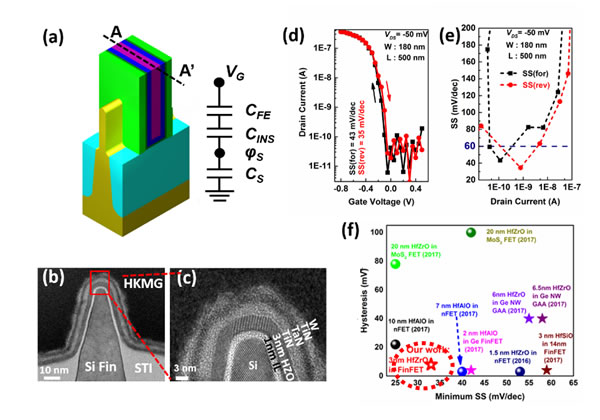
Recently, the Integrated Circuit Pilot Technology R & D Center of the Institute of Microelectronics, Chinese Academy of Sciences, targeting the performance requirements of high-performance and low-power transistors at 5 nanometers and below, is based on mainstream post-high-K metal gate (HKMG-last) 3D FinFET device integration technology and has succeeded Developed a high-performance negative-capacitance FinFET device. Existing silicon-based transistors are limited by Boltzmann thermodynamics, and the sub-threshold swing SS at room temperature is greater than or equal to 60 mV / dec, which prevents the operating voltage from continuing to decrease. When integrated circuit technology enters the node of 5 nanometers and below, with the continuous increase of integration, it faces serious challenges of sharply increasing power consumption while maintaining device performance. Based on the mainstream post-HKMG FinFET integration process, the team of researcher Yin Huaxiang of the Pilot Center, through material process optimization and multi-gate device capacitance matching design, combined with high-quality and low-interface state 3 nanometer hafnium zirconium metal oxide film, developed an excellent NC -FinFET devices, achieving 500-nanometer gate length NCs with SS and threshold voltage hysteresis of 34.5mV / dec and 9mV, respectively, and 20-nanometer gate length NCs with SS and threshold voltage hysteresis of 53mV / dec and 40mV, respectively -FinFET devices. Among them, the drive current of the 500-nanometer gate-length NC-FinFET device is 260% higher than that of the conventional HfO2-based FinFET device (non-NC-FinFET) and the current switching ratio (Ion / Ioff) is greater than 1x10⁶, marking the new NC-FinFET where Microelectronics is located. New progress has been made in the development of devices. The above research results were published in IEEE Electron Device Letters (DOI: 10.1109 / LED.2019.2891364), an international journal in the field of microelectronic devices, and quickly received high attention from many international R & D institutions. The innovative research on the integrated circuit pilot process was supported by the National Science and Technology Major Project 02 and the National Key R & D Program. Figure: (a) Basic structure of negative capacitance FinFET; (bc) Three-dimensional device channel structure and ferroelectric HZO film structure; (de) Device IV and SS characteristics; (f) International comprehensive comparison of latest device performance (SS and hysteresis) The lower the voltage, the better) Single Basin Faucet,Bathroom Basin Faucets,Single Hole Basin Tap,Single Handle Basin Faucet AIHUI Sanitary Ware , https://www.fsaihuisanitary.com